Versa Cluster Platform
Our Versa cluster platform is an automated front-end option for high-volume manufacturing that enables greater production efficiency to meet higher throughput requirements.
Learn MoreA semiconductor is a material which conducts electricity more than an insulator, such as glass, but less than a pure conductor, such as copper. Their conductivity can be altered to meet the specific needs of the electronic component in which it resides. Semiconductors can be found in thousands of products such as computers, smartphones, appliances, and medical equipment.
Silicon semiconductors are used in virtually every electronic device and component, but compound semiconductors are growing globally as well. They are critical in optical applications like light-emitting diodes (LEDs), photodetectors, IR detectors and focal plane arrays. Some, like focal plane arrays, are low-throughput applications. Due to growing consumer demand, many of these applications, such as RF power transistors in cell phones, require high-volume manufacturing.
Common semiconductor applications include contact metallization, under bump metallization, barrier overcoats, insulators, and low damage etch, as well as a wide array of specialty applications including thin film resistors, resonators, and optical coatings. Denton Vacuum offers high-quality and consistent deposition and etch solutions for all of these semiconductor coating applications.
![]()
The semiconductor market is a $300B+ industry driven by strong demand for IT, sensors, and consumer devices. The competitiveness of the industry lies with a heavy focus on R&D to make chips smaller, faster, and more functional, as well as cost-effective for high-volume manufacturing.

Sensors convert changes in a physical parameter into electrical signals which can be monitored and acted upon by an electronic device. Applications range from monitoring airspeed, temperature, and humidity to reducing interference in cell phone signals. The simple structure of thin film sensors reduces their cost of manufacture and improves their accuracy and reliability, even under the harshest operating conditions.

Power semiconductors control and convert electricity in electronic systems. Coming in the form of amplifiers, switches, and diodes, these devices are increasingly critical in industries such as renewable energy, automotive, and aerospace. Denton offers the most comprehensive production platforms and application solutions supporting the needs of power device manufacturing.
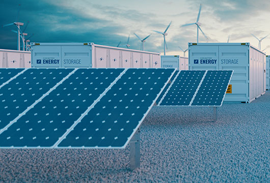
Nothing in the 21st century world of electronics would be possible without electrical power, and thin film technologies are behind all of it. From superconductor wire used to improve the efficiency of power transmission, to flexible batteries, multi-layer capacitors, and fuel cells used in mobile devices and electric cars, Denton Vacuum’s thin film deposition systems are featured solutions for energy storage and transmission devices.
Extreme UV light (EUV) has wavelengths between 5 and 50 nm, which are much shorter than ultraviolet wavelengths. EUV lithography is required for semiconductor line widths less than 9nm, and one primary application this is used for in semiconductor production is pattern etching. As feature sizes get smaller, EUV’s short wavelengths are needed to meet requirements for 7nm semiconductors processing, and due to the small feature size, extremely low particle counts on the mask blanks are necessary.
As semiconductor device architectures continue to shrink and conventional deposition technologies reach their fundamental limits, ion beam deposition and ion beam etch are under investigation for manufacturing the next-generation chip technology. Denton Vacuum has solutions for advanced semiconductor applications ranging from low resistivity contacts to ultrathin barriers and low damage etch.
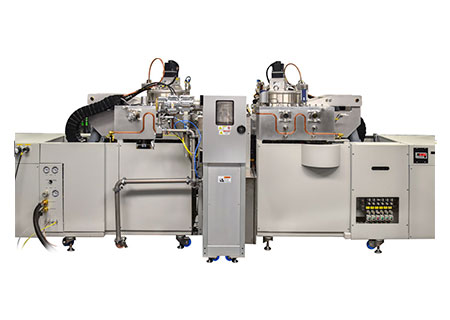
Our Versa cluster platform is an automated front-end option for high-volume manufacturing that enables greater production efficiency to meet higher throughput requirements.
Learn More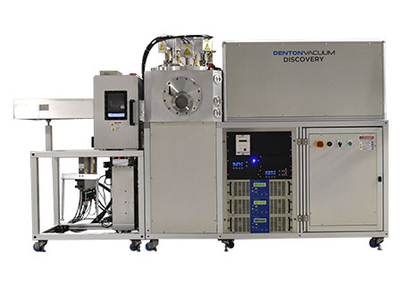
Magnetron sputtering is a highly versatile thin film deposition technique for coating films with excellent adhesion and high density. It is often chosen for the deposition of metallic and insulating coatings that have specific optical or electrical properties. Denton’s proprietary Isoflux Cylindrical Magnetron is able to deposit very thin, very uniform films of ion beam deposition quality.
Learn More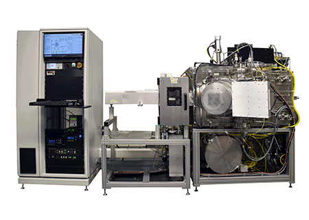
Denton Vacuum has developed proprietary solutions for ion beam sputtering that provide stable deposition rates for excellent film thickness and uniformity control. It also enables low damage etch and is optimized to meet your exact needs and specifications.
Learn MoreDue to the complex and intricate nature of semiconductors, failures in integrated circuits (IC) happen for a variety of reasons. Semiconductor failure analysis is the process of determining how or why these failures in the devices have occurred. Failure analysis is necessary in order to understand what caused the failure and how it can be prevented in the future.
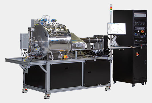
The first step in any failure analysis project is to isolate the source of the failure. If that failure is happening in one specific system, isolate that system. Later, using investigative failure testing equipment, you can identify the particular IC causing the fault. That’s where Denton’s Infinity Failure Analysis system comes into play.
The Infinity FA system is a high-performance ion beam etching tool designed for failure analysis sample preparation, critical thin film profiling, and delayering in semiconductor manufacturing. The system includes a robust SIMS package for analyzing thin film removal, is ESD compliant, and is fully computer-controlled for high automation and repeatability.

The change from 4G to 5G will bring higher power consumption requirements which means sophisticated semiconductors to make the chips. With 5G becoming more mainstream, the demand for lasers, filters, and power amplifiers will drive higher production levels.

A semiconductor controls and manages the flow of electric current in electronic equipment and devices. Semiconductors can be found in a wide range of power devices ranging from superconductor wire used to improve the efficiency of power transmission, to flexible batteries, multi-layer capacitors, and fuel cells used in mobile devices.

Semiconductors enable clean, renewable energy sources and improve energy efficiency. They are used to condition power from solar and wind so the energy can be used in equipment or the electric grid. Denton offers the most comprehensive high volume production platforms and application solutions supporting the needs of energy-related manufacturing.
![]()
There are two different types of diode lasers, edge-emitting lasers (EELs) and vertical cavity surface emitting lasers (VCSELs). Both are well established in the opto-electronics and semiconductor markets, and, as the technology matures, they enable innovation in next-generation products.
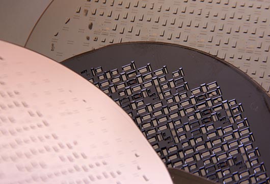
A semiconductor-based temperature sensor measures temperature with temperature-sensitive voltage and current characteristics. Sensors give a linear output by using thin films as the sending component to measure the relative humidity of an environment. Current MEM products include display chips, optical switches, and more.
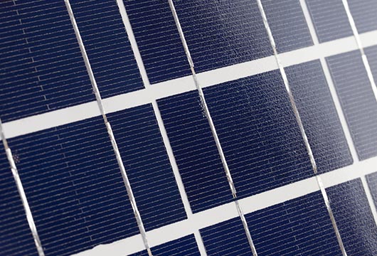
Much like the use in clean energy, semiconductors in solar panels absorb light and transfer energy to the layers that send electrical currents to the power grid. Semiconductors are key to their functioning and low-emission products like solar panels help minimize climate impact.