Posted on
To form indium bumps, a patterned mask is applied to the wafer and then indium is deposited. The patterned mask has “holes” that allow some indium to deposit directly onto the wafer, while the rest of the indium is deposited onto the mask. After indium bump deposition, the unwanted indium and the mask must be removed. This is known as lift-off.
If the indium is not deposited properly, indium bumps could be unintentionally removed. This results in dead pixels or unmade connections on the focal plane array. However, when those connections are ensured, device yield greatly improves.
Balancing Bump Quality with High Pixel Density
Patterned coatings are an important requirement for forming interconnects in flip-chip micro arrays. Using indium as the coating material, the indium is deposited on an array of under-bump metallization (UBM) layers, which connect through a sensor device. A similar process is repeated on a controller device. The indium bumps form interconnects between the sensor and the controller to create a single photodetector device.
There is increasing demand for improved bump quality with high aspect ratio arrays, to meet requirements for higher pixel densities in newer applications with smaller feature sizes. These tight requirements make it more difficult to form good bumps during deposition. With good bump formation, the lift-off process will reveal high quality bumps that deliver high device yield.
Indium can be deposited at room temperature, but to create small diameter bumps (e.g., less than 10 µm) with a high aspect ratio (above 1:2 height to width), you need to use a cryo-cooled chuck. The cryo-chuck creates good shear strength and crystal structure, but adding this to your process can introduce new yield loss due to lack of bump adhesion. These missing bumps will result in dead pixels on the photodetector device.
To find the right balance between good bump formation and adhesion, you need to optimize your process to improve lift-off yield.
What is the Lift-Off Process?
This refers to the process of removing the masking agent (typically a photoresist) as well as the unwanted indium, leaving behind the bump arrays across the photo detector device. This is what ultimately creates the pixels for focal plane arrays, after the indium is actually deposited. Poor adhesion to the under-bump metallization lead to poor lift-off, which negatively affects device yield.
How Does Pre-Cleaning Improve Lift-Off?
Pre-cleaning is a thin film deposition process that can greatly improve adhesion and lead to much better lift-off. It is performed before indium bump deposition, and it is done to ensure that the bump formations remain intact after lift-off, even at cryogenic temperatures.
As the name implies, during pre-cleaning, the surface of the substrate is thoroughly cleaned to remove any microscopic particles or molecules that might come between the substrate surface and the coating, such as water. At cryogenic temperatures, the water is much more likely to stick to the substrate during deposition, so the pre-cleaning step is imperative to removing these molecules and ensuring good adhesion.
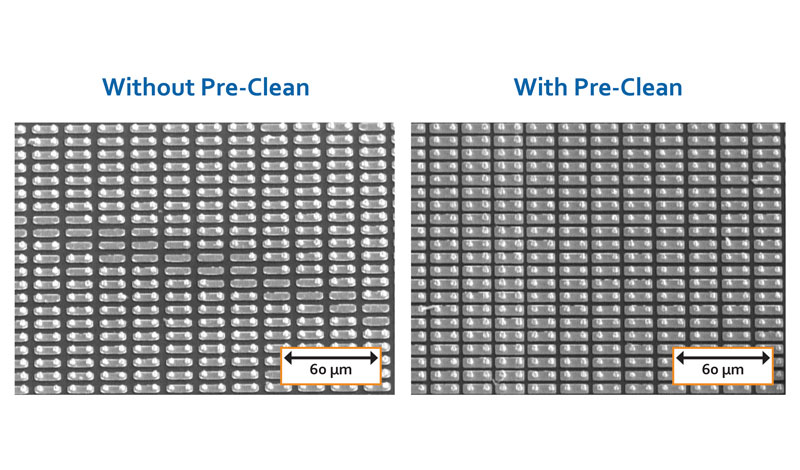
Denton Vacuum’s research has shown significant improvements in bump formation and device yield when pre-clean is performed before indium bump deposition. Despite using the same photoresist process and being deposited under the same conditions, the data clearly shows that without pre-clean, there were a number of bumps missing from the array after lift-off, and with pre-clean, the bumps stayed intact.
There are a number of considerations to take into account before selecting a particular pre-clean method. Denton’s proprietary pre-clean is integrated into our application-specific indium bump system, and provided as part of our integrated indium bump solution. You can read more about attaining good bump formation during indium bump deposition in our infographic.