See how Denton Vacuum has pioneered thin film for 6 decades.

A Look Ahead at the Semiconductor Industry

2 robotic arms manufacturing a semiconductor

Posted on

Semicon West 2022 connected business and technology leaders, researchers, and industry analysts from across the microelectronics supply chain in California and online for their annual event. Here are some key takeaways from the conference. Semiconductor Market on Track to a Trillion The semiconductor industry faced several recent challenges and has seen disruptions. A crisis response… Read More

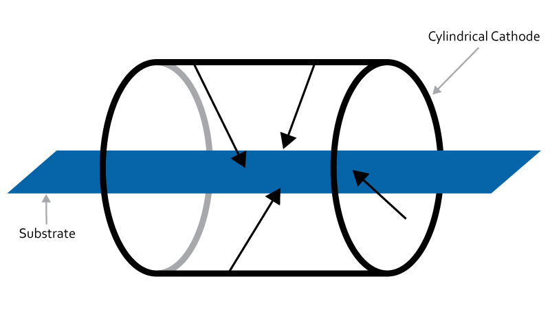
Isoflux: The Optimal Choice for Ultrahigh Uniformity Flat Substrates

Diagram showing a cylindrical cathode configuration with the substrate inside the cathode, sputtering inward.

Posted on

Inverted cylindrical magnetron (ICM) sputtering is the optimal choice for applications that require ultra-uniform coatings on flat substrates. For example, ICM sputtering offers uniformity below 1% on standard 200mm wafers. ICM sputtering follows the same steps as conventional magnetron sputtering except a cylindrical cathode is used instead of a planar cathode. Instead of sputtering up… Read More

The Basics of Ion Beam Delayering

Posted on

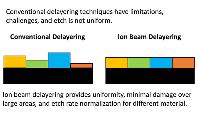
What is Ion Beam Delayering? Ion beam delayering is the removal of material one layer at a time from a substrate using ion beam etch techniques. The primary objective in the delayering process is to remove material in a manner that exposes the defect location which is buried underneath the layers. As semiconductor device nodes… Read More

How to Handle Varying Wafer Sizes in Compound Semiconductor Manufacturing

A central wafer handler, with a wafer carrier, holds a semiconductor wafer and moves it between deposition chambers.

Posted on

In large-scale, high-volume silicon semiconductor production, such as for microprocessors and DRAM, manufacturers often prefer direct handling of wafers during the thin film deposition process. This makes perfect sense for mass-producing wafers that are all 300mm in size. However, in the compound semiconductor industry, multiple wafer sizes are quite common. It is not economically viable… Read More

Achieving Repeatability in High-Volume Manufacturing

Posted on

Repeatability is a key factor in any production process. Along with uniformity, it ultimately determines the yield of any thin film deposition process. When designing a thin film system configuration for high-volume manufacturing, repeatability becomes especially paramount. Why is Repeatability Important? Accuracy (hitting the middle of a spec) and precision (repeatable results) are the two… Read More

Thin Film Considerations for High-Volume Manufacturing

Posted on

To scale smoothly into high-volume manufacturing, you need to be prepared to meet higher throughput requirements without impacting your process control. This means investing in the right thin film system configuration to meet your demanding throughput needs. Factors to Consider When selecting a thin film deposition system for high-volume production, there are a number of… Read More

Selecting the Right Front-end Option

Two employees in hazmat suits in a high-tech manufacturing environment

Posted on

If you’re looking to improve productivity in your sputtering process, there are several front-end options available to use. When paired with a compatible standard sputter chamber, these front-end options can be used to increase throughput and production efficiency while providing consistent, repeatable results. Front-end Options Single Chamber, Single Wafer Loadport: This type of front-end option… Read More

Thin Film Solutions for the Semiconductor Market

Semiconductors shown through a phone screen

Posted on

By the end of 2018, the semiconductor industry is expected to grow to $451 billion, an increase of 7.5% from 2017. With more innovative technology and electronic devices expected to reach the market within the next five to 10 years, semiconductor manufacturers should prepare for growth and examine production solutions for future applications, including thin… Read More