See how Denton Vacuum has pioneered thin film for 6 decades.

Phoenix: Large Area Coating System for In-Line Production

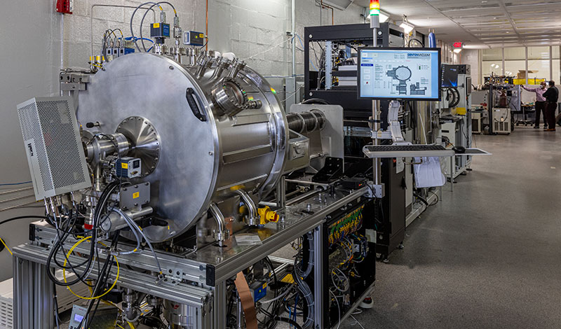
A close up of the Denton Vacuum Phoenix system

Posted on

Denton’s Phoenix system platform is designed for high-volume in-line production. The system comes in two primary configurations: the Phoenix LC for magnetron sputtering with a rectangular or rotary linear cathode, and the Phoenix PIB-CVD for room-temperature chemical vapor deposition. Both systems can be configured with multiple sources to support a variety of applications. In this… Read More

5 Benefits of PIB-CVD Over PE-CVD

Woman's hands holding a cell phone

Posted on

Thin films obtained by standard chemical vapor deposition (CVD) typically require temperatures ranging from 600°C to 800°C. Using plasma enhanced CVD (PE-CVD) allows reactions to occur at temperatures down to 350°C. Plasma ion beam CVD (PIB-CVD) advances this process even further by allowing room temperature deposition. Without the need to heat a substrate to such… Read More

Ion Beam Etch for Semiconductor Failure Analysis

A wafer being placed inside of an Infinity FA system.

Posted on

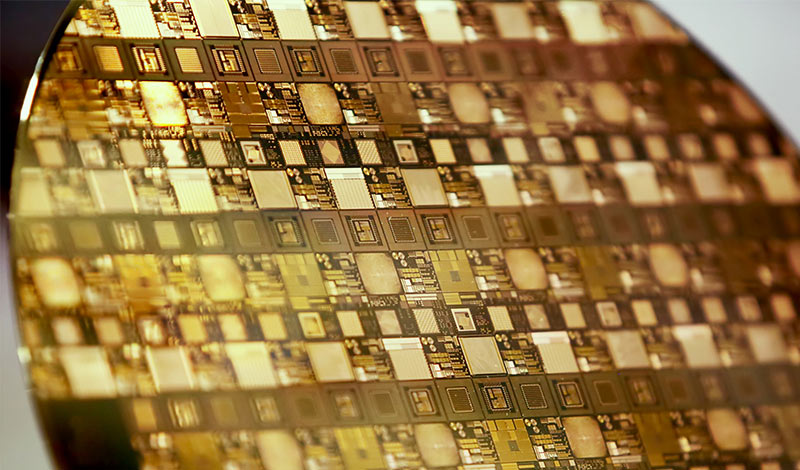
Conventional failure analysis methods have failed to scale with modern semiconductors, which are larger, more complex, and incorporate a wider variety of materials than ever before. Ion Beam Etch, or IBE, overcomes the challenges that conventional failure analysis methods cannot.  IBE provides a uniform etch no matter the material, exposes large areas of interest with… Read More

Utilizing Plasma in Chemical Vapor Deposition: Plasma Enhanced CVD vs PIB-CVD

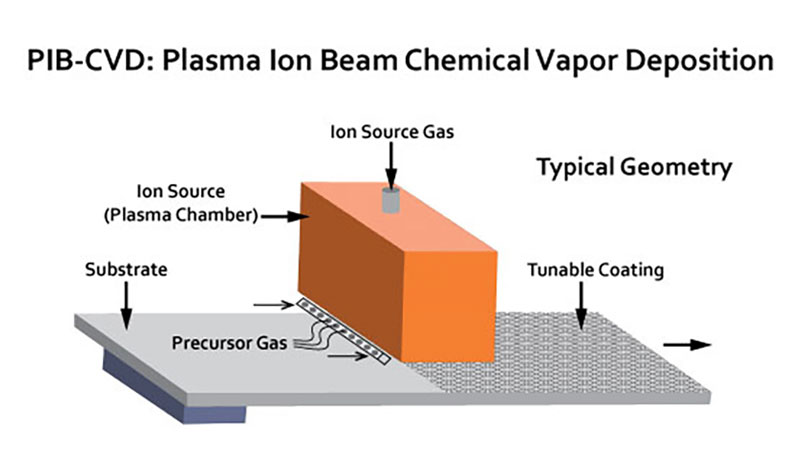
Plasma Ion Beam Chemical Vapor Deposition

Posted on

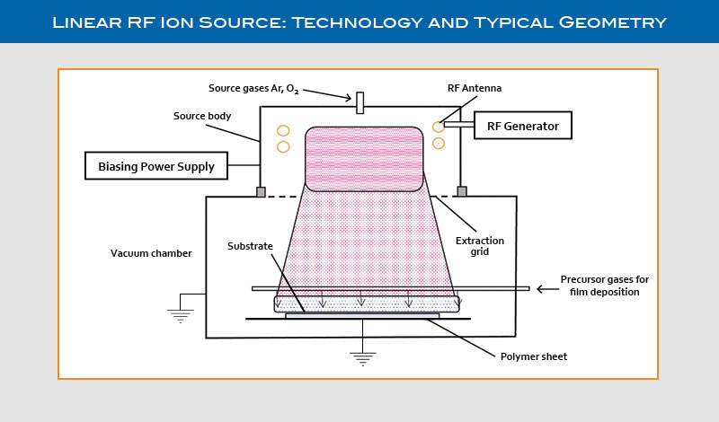
In thin films obtained by Chemical Vapor Deposition (CVD), chemical reactions are driven by applying heat to the substrate to be coated or to the area immediately around the substrate. Reactive precursor gasses are then introduced into the deposition chamber and react immediately with the heated substrate surface or combine to form new compounds that… Read More

How Can You Improve Factory Throughput in Thin Film Deposition?

Close up image of a silicon wafer

Posted on

Factory throughput in thin film deposition is one of the most critical factors affecting overall production performance. Whether you are manufacturing for high or low volume applications, you need to be able to meet production needs in the most cost-effective way possible, and scale into higher production when needed. Finding ways to raise your factory… Read More

4 Industry Applications for PIB-CVD

Posted on

In the world of thin film deposition, there are few techniques that have the versatility of PIB-CVD. Short for plasma ion beam assisted chemical vapor deposition, PIB-CVD is a cutting-edge thin film deposition process that can be used to deposit large area multifunctional thin films with greater efficiency as well as engineer new materials.  What… Read More

The Customer Application Development Center at Denton Vacuum

Posted on

Welcome to the Denton Vacuum Applications Laboratory Denton Vacuum has hit a milestone with the Customer Application Development Center, the Apps Lab, as we pass the 10-year mark. The CADC empowers innovation by producing state-of-the-art sputtered, etch, and evaporated thin films and evaluating machine performances with our cutting-edge tools. In the CADC, Denton has three… Read More

Denton Vacuum Infinity FA Tool

Posted on

Enable uniform removal of the entire layer regardless of chemical composition The Infinity FA from Denton Vacuum is optimized for delayering applications. The Infinity FA can utilize multiple etch technologies for uniform removal of layers. This high-performance etch tool is designed for delayering finished or in-process integrated circuits for failure analysis or reverse engineering. Learn… Read More

Why Semiconductor Manufacturers Prefer Denton’s Collaborative Approach

Posted on

Semiconductor manufacturing often takes a hardware-centric perspective when selecting equipment and vendors. However, manufacturers can benefit from a vendor’s industry experience and, instead, take an application-specific route. A partner like Denton Vacuum, with decades of experience, can address key concerns to get you to production faster than piecing together OEM parts. Working with a single vendor, or… Read More

SIMS Analytics for Semiconductors

Posted on

Secondary ion mass spectroscopy (SIMS) is a technique for compositional analysis of solid surfaces (such as semiconductors) in which material is removed from a surface by ion beam sputtering and the resultant positive and negative ions are analyzed in a mass spectrometer. This technique can be used to analyze the composition of semiconductor devices and… Read More