See how Denton Vacuum has pioneered thin film for 6 decades.

Improving Adhesion During Lift-Off For Indium Bump Deposition

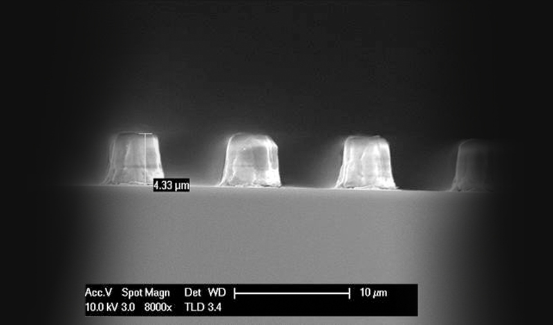
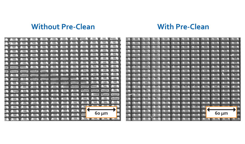
Side-by-side comparison of indium bump arrays without pre-clean and with pre-clean, respectively.

Posted on

To form indium bumps, a patterned mask is applied to the wafer and then indium is deposited. The patterned mask has “holes” that allow some indium to deposit directly onto the wafer, while the rest of the indium is deposited onto the mask. After indium bump deposition, the unwanted indium and the mask must be… Read More
4 Design Considerations for Improving Lift-Off Yield

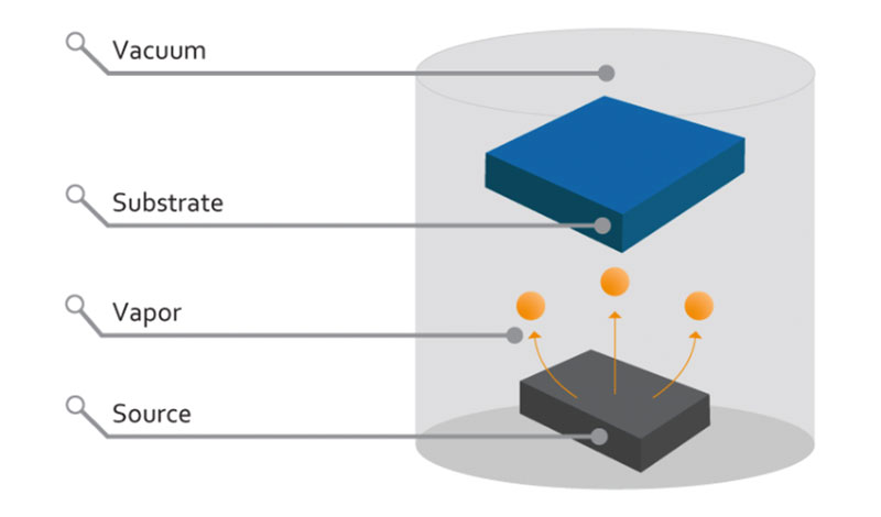
substrate graphic

Posted on

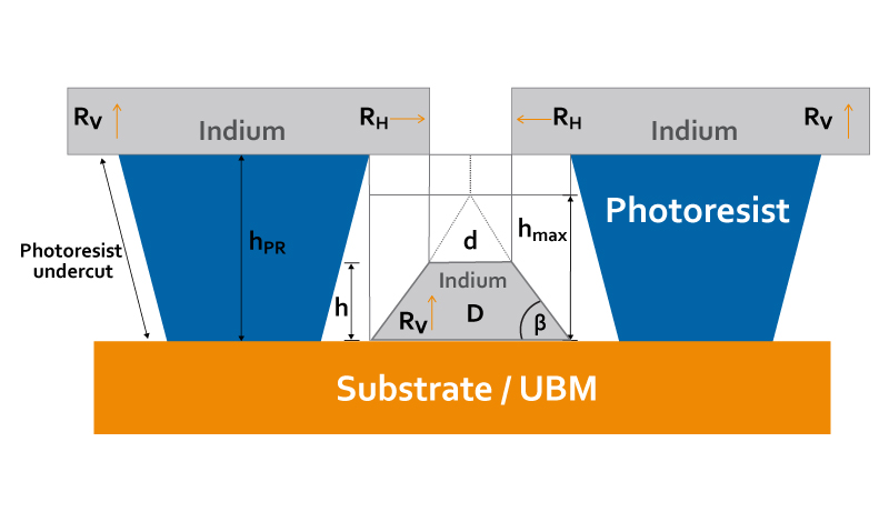
While thin film deposition is often used to create a continuous coating on a substrate, there are many applications where a patterned coating is required. These patterns create bumps, trenches or ridges across the surface of the substrate. This coating type is used for 3D applications, such as electrical interconnects. Focal plane arrays with high-density… Read More

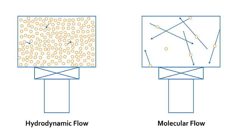
Which High Vacuum Pump is Best for PVD?

hydro molecule diagram

Posted on

Physical vapor deposition (PVD) and other types of thin film deposition require a vacuum chamber to create thin film coatings. A vacuum is created when the coating chamber is pumped down, and all of the air molecules and other gasses are evacuated from the system. If these molecules are not reduced to an acceptable level,… Read More

Using Ion Sources in Thin Film Deposition

Posted on

To create more precise thin films, manufacturers often include an ion source to their thin film deposition system configuration. By using an ion source, manufacturers can produce an ion species that has specific properties during deposition. The source controls the energy, trajectory and reactivity of the ions it produces, helping to create a thin film… Read More

Increasing Throughput in Sputtering and Evaporation

Posted on

As integral as throughput is when it comes to meeting production needs, there is no single answer for improving throughput, especially across different deposition methods. With both evaporation and magnetron sputtering, there are a number of factors you need to consider in order to raise your total throughput. Improving Throughput in Magnetron Sputtering With a… Read More

Weighing the Benefits of Sputtering vs. Evaporation

Posted on

When comparing the four main types of physical vapor deposition (PVD) for thin films, it is important to know the benefits and drawbacks of each before you decide which method will best suit your application. PVD can occur through sputtering (magnetron or ion beam), which utilizes energetic ions colliding with a target to eject (or… Read More

Closure Rate and Uniformity in Indium Bump Deposition

indium bump deposition

Posted on

In indium bump deposition, there is a tradeoff between closure rate and closure uniformity. A slower closure rate and high closure uniformity is ideal, but often, the closer you get to your desired specs in one area, the more you sacrifice with the other. Closure Rate vs. Closure Uniformity Closure rate: This refers to the… Read More

Which Type of Thin Film Coating is Best?

A person pressing on a touchscreen display.

Posted on

Thin film coatings serve a number of purposes for different applications, including across the opto-electronics, display, semiconductor and medical fields. Here is a quick rundown of a number of common coatings that are available, their properties, and the applications they’re optimized for in order to help you figure out the best coating for your performance… Read More

Differences in Grain Size Between Deposition Methods

Close up of gold panning pan with sifting sand.

Posted on

Grain size refers to the size of the individual crystallites or particles that compose a solid metal. Grain size, as well as the boundaries between the grains, are important factors for determining physical properties of the entire metal. In thin film deposition, if the particles are deposited with high energy, and there is a high… Read More

Considerations for Indium Bump Deposition

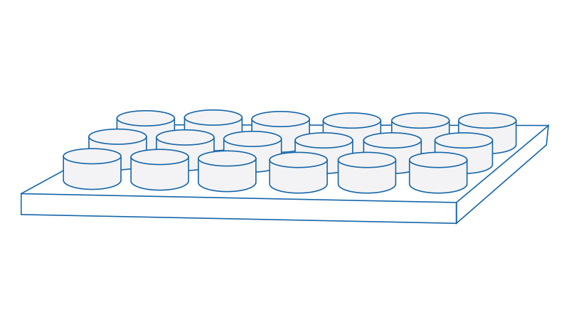
indium bump drawing

Posted on

With today’s technological advances, higher pixel density in focal plane arrays is a necessity as demand for improved visual quality goes up. Because of this, feature sizes on focal plane arrays are getting smaller, which requires higher density interconnects to bond the detector array to the readout chip. The current electroplating process just can’t deliver… Read More