The Basics of Ion Beam Delayering
Posted on
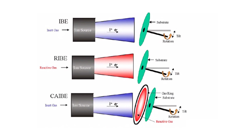
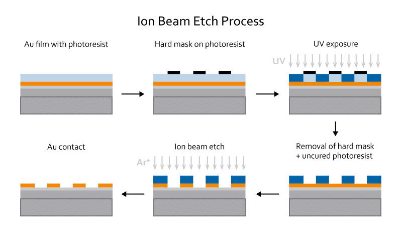
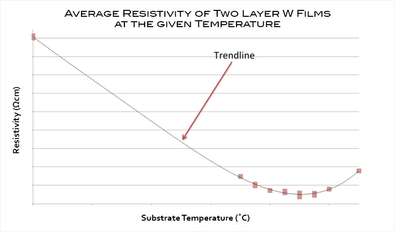
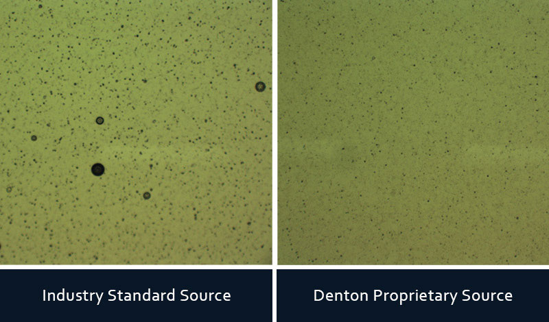
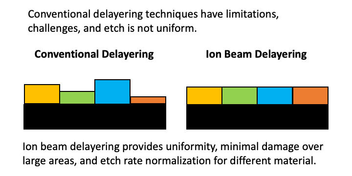
What is Ion Beam Delayering? Ion beam delayering is the removal of material one layer at a time from a substrate using ion beam etch techniques. The primary objective in the delayering process is to remove material in a manner that exposes the defect location which is buried underneath the layers. As semiconductor device nodes… Read More