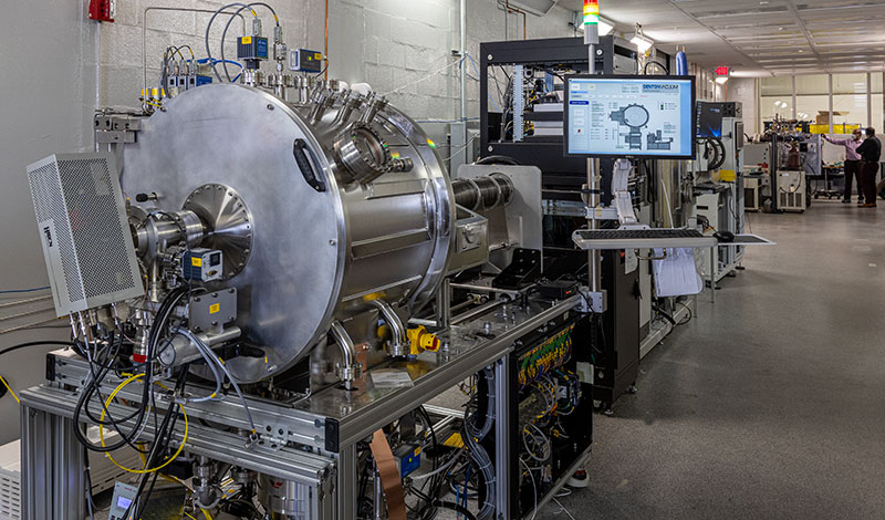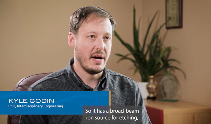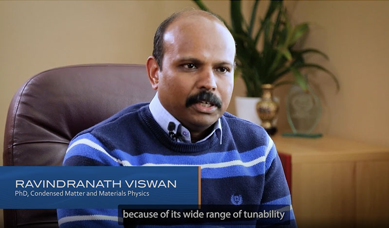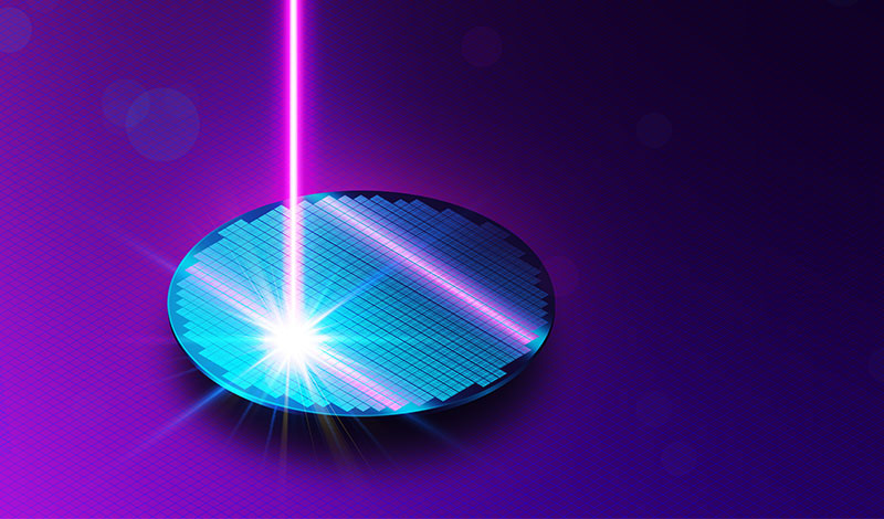
See how Denton Vacuum has pioneered thin film for 6 decades.

The Denton Difference: 4wave Acquisition Bolsters Denton Vacuum as Global Nanotechnology Leader

Posted on

Forward Thinking There is a need for innovative nano-engineering solutions in the rapidly growing markets of cloud computing, data storage, telecommunications optics, high-power electronics, and sensors for the IoT. Denton’s breadth of technologies and market focus enable advancements ranging from applications in semiconductor failure analysis to production solutions for IR detectors, semiconductor lasers and precision… Read More

Considerations for Deposition of Multi-Layer IR Bandpass Filters

Graph depicting the relationship between transmission and wavelength in IR bandpass filters

Posted on

What are Infrared (IR) Bandpass Filters An optical bandpass filter (BPF) is a device that passes wavelengths within a certain range and blocks wavelengths outside that range. One prominent type is infrared (IR) bandpass filters which are used in a wide range of applications including thermal imaging (night vision), emission monitoring for power plants and… Read More

The Basics of Ion Beam Delayering

Posted on

What is Ion Beam Delayering? Ion beam delayering is the removal of material one layer at a time from a substrate using ion beam etch techniques. The primary objective in the delayering process is to remove material in a manner that exposes the defect location which is buried underneath the layers. As semiconductor device nodes… Read More

3 Techniques for Ion Beam Etching

Ion Beam Etch (IBE), Reactive Ion Beam Etch (RIBE), and Chemically Assisted Ion Beam Etch (CAIBE)

Posted on

In ion beam etching, a type of dry etching, an ion source is used to remove material from a substrate. This process can be used to create device components and nanostructures, such as in integrated circuits and other semiconductor applications. To enable high yield and meet performance requirements, your application may require different etch technologies…. Read More

Denton Receives Patent for Linear Plasma Ion Source

A CAD drawing of Denton Vacuum's patented linear plasma-ion source.

Posted on

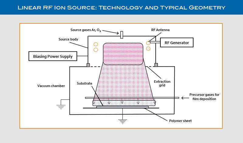
Denton Vacuum was recently assigned U.S. patent number 10,815,570 for a linearized energetic radio-frequency plasma ion source. This source is designed as a large area, filament-free source that is fully compatible with high-throughput, in-line sputtering systems. Some of the unique, patent-protected features of this source are: Plasma ion source with independent control over ion current… Read More

What is Ion Beam Etching?

Diagram showing the step-by-step process for creating gold contacts using ion beam etch.

Posted on

Ion beam etching (IBE) is a thin film technique that utilizes an ion source to carry out material removal processes on a substrate. IBE is a type of ion beam sputtering and, whether it’s used for pre-clean or patterned etching, it helps ensure excellent adhesion and precise formation of 3D structures. Benefits of Ion Beam… Read More

Thin Film Requirements for Emerging Display Applications

A 3D rendering of a foldable smartphone, showing the lock screen with the date in the left panel and the time in the right panel.

Posted on

As manufacturers look to introduce exciting new features to customers and increase device lifespan in consumer electronics applications, thin film coating requirements are beginning to change as well. Durability and performance continue to be critical but flexibility and ultra-thin coatings are increasingly in demand. Emerging display applications are seeing new form factors and a heavy shift… Read More

Reducing Resistivity and Stress in Tungsten Coatings

Graph showing the average resistivity of two layer W films at the given substrate temperature.

Posted on

Tungsten coatings are commonly used in semiconductor applications and have the potential to be used in emerging solar energy applications. These thin films are commonly subject to high stress and low adhesion, but when manufacturers try and compensate for stress, it leads to increased resistivity. In order to achieve the best performance and repeatability for… Read More

Managing Spit Defects During Evaporation

A side-by-side comparison of spit during evaporation with a standard source design, and with Denton's proprietary source design. With Denton's design, you see significantly less spit particles.

Posted on

Spit defects are some of the biggest obstacles to ensuring thickness uniformity and production efficiency in evaporation and indium bump deposition. There are ways to adjust your process to eliminate spit defects and improve yield, but if you work with a partner who has solved for these defects in their system design, you will realize… Read More

Enhancing Thickness Uniformity for Medical Device Coatings

Surgeons inserting a stent during heart surgery.

Posted on

Medical devices often require thin film coatings to optimize performance and longevity, while also ensuring patient safety. Because these devices often feature unique properties compared to “normal” substrates, such as a completely curved or flexible structure, they have challenging thin film deposition process requirements. Magnetron sputtering with an inverted cylindrical cathode is one thin film… Read More