See how Denton Vacuum has pioneered thin film for 6 decades.

Phoenix: Large Area Coating System for In-Line Production

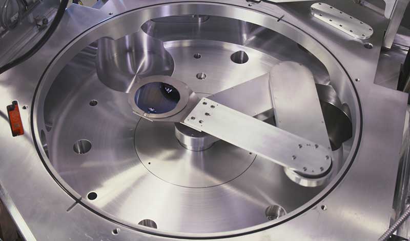
A close up of the Denton Vacuum Phoenix system

Posted on

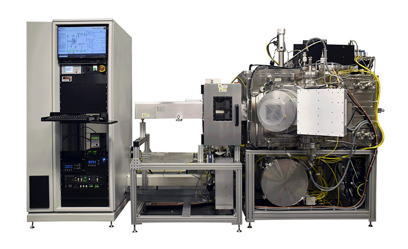
Denton’s Phoenix system platform is designed for high-volume in-line production. The system comes in two primary configurations: the Phoenix LC for magnetron sputtering with a rectangular or rotary linear cathode, and the Phoenix PIB-CVD for room-temperature chemical vapor deposition. Both systems can be configured with multiple sources to support a variety of applications. In this… Read More

5 Key Considerations for Pre-Cleaning

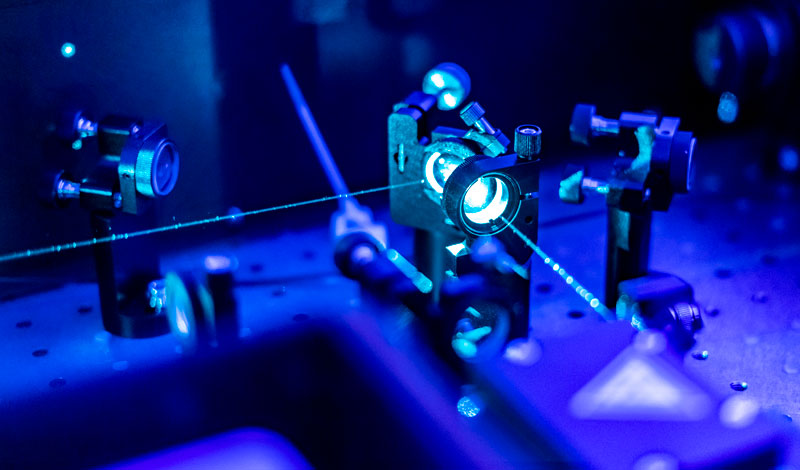
A close up of lasers working on a chip

Posted on

In order to achieve the desired properties and meet performance requirements, substrates may need to be pre-cleaned prior to deposition. While there are several methods that can be used to carry out this process, each has its own benefits depending on your pre-cleaning goal and deposition process. For example, RF glow plates use lower energy… Read More

5 Benefits of PIB-CVD Over PE-CVD

Woman's hands holding a cell phone

Posted on

Thin films obtained by standard chemical vapor deposition (CVD) typically require temperatures ranging from 600°C to 800°C. Using plasma enhanced CVD (PE-CVD) allows reactions to occur at temperatures down to 350°C. Plasma ion beam CVD (PIB-CVD) advances this process even further by allowing room temperature deposition. Without the need to heat a substrate to such… Read More

Ion Beam Etch for Semiconductor Failure Analysis

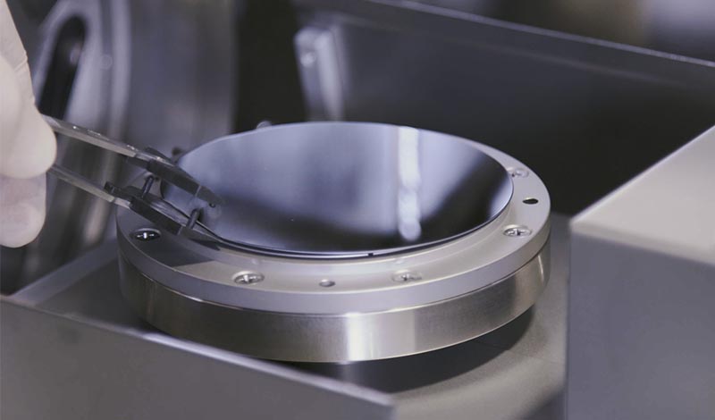
A wafer being placed inside of an Infinity FA system.

Posted on

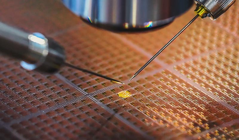
Conventional failure analysis methods have failed to scale with modern semiconductors, which are larger, more complex, and incorporate a wider variety of materials than ever before. Ion Beam Etch, or IBE, overcomes the challenges that conventional failure analysis methods cannot.  IBE provides a uniform etch no matter the material, exposes large areas of interest with… Read More

What is Magnetron Sputtering?

Magnetron Sputtering

Posted on

Magnetron sputtering is a plasma-based technique for physical vapor deposition (or PVD) coating that creates dense films with good adhesion. It is excellent for depositing materials with high melting points that cannot be evaporated, and it has the highest scalability of any PVD type. Magnetron sputtering provides excellent precision in film thickness and density of… Read More

Bias Target Sputtering for Thin Film Deposition

Laser reflecting on optic table

Posted on

Traditional ion beam sputtering (IBS) provides excellent control over ion energies and thin film stoichiometry, making it the process of choice for sputtering metals and dielectrics for applications such as vanadium oxide microbolometers and VCSELs. Still, IBS has various challenges in meeting the necessary standards for applications in which a high degree of precision and… Read More

Cathode Options for Magnetron Sputtering

Denton Vacuum magnetron sputtering illustration

Posted on

Magnetron sputtering is a versatile deposition technique that creates very dense films with good adhesion. It can easily deposit materials with high melting points that cannot be evaporated. Denton Vacuum’s magnetron sputtering systems are highly configurable with multiple cathode options to meet the specific requirements of different applications.  In this article, we discuss the multiple… Read More

Is Evaporation or Sputtering Better for Your Application?

Robotic arm adding an OLED screen to a smart phone

Posted on

When selecting a physical vapor technique for your manufacturing process, the end application will greatly affect which technique is best. While PVD has many forms, there are two prominent techniques: evaporation and sputtering. Sputtering through magnetron or ion beam (IBS) utilizes energetic ions colliding with a target to eject (or sputter) target material. Thermal resistive… Read More

How to Prevent Defects in Thin Film Sputtering and Evaporation

Two men in sterile suits

Posted on

The goal of any thin film deposition method is to create a high-quality uniform film across the entire surface of a substrate. Unfortunately, defects such as spits, particles, and voids can interfere with your ability to reach desired film quality. If necessary, there are ways to adjust a manufacturing process to eliminate such defects and… Read More

Vertical Cavity Surface Emitting Lasers (VCSELs) and their Applications

GaAs VCSEL diagram

Posted on

Lasers are used in a wide variety of everyday applications, in everything from fiber optic telecommunications, to computer mice, to cell phones, and even cars. This is made possible by semiconductor lasers, particularly by vertical-cavity surface-emitting lasers (VCSELs). A VCSEL is created from a complex multilayer structure that is formed by depositing thin film layers… Read More