Posted on
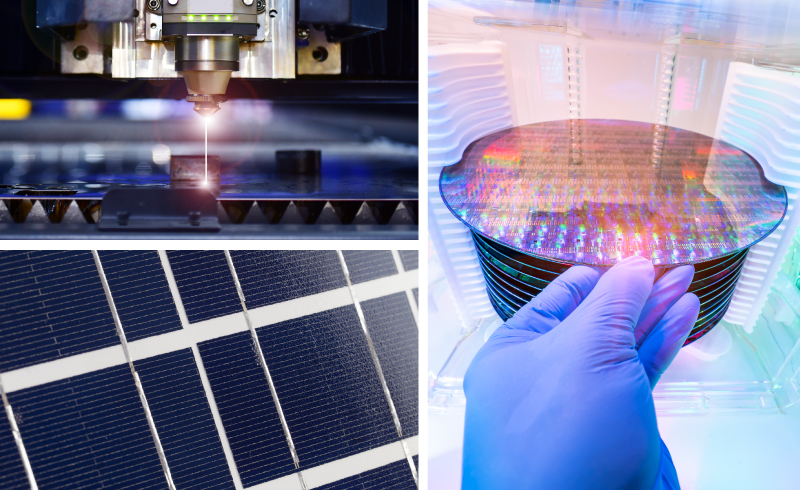
Many of today’s electronic devices are based not on silicon semiconductors – the mainstay of the computer industry for decades – but on III-V semiconductors, built using specialized alloys with unique properties. However, the inherent cost, brittle nature, and unique characteristics of III-V semiconductors often demand special material handling during the manufacturing process. Denton offers thin film solutions that meet these challenges.
Why III-V Semiconductors Are So Useful
III-V semiconductors are alloys of elements from groups III and V of the periodic table. Group III includes elements like boron (B), aluminum (Al), gallium (Ga), and indium (In), while group V includes elements like nitrogen (N), phosphorus (P), arsenic (As), and antimony (Sb).
What makes III-V semiconductors so useful is they have a direct bandgap, enabling them to directly convert photons to electrons (and vice versa). They also offer better thermal conductivity and electrical efficiency than silicon. III-V semiconductors are well-suited for applications such as:
- Optoelectronics: LEDs (Light Emitting Diodes), lasers, photodetectors, and sensors
- Photovoltaics: Flexible and lightweight III-V thin-film solar cells
- Electronics: High-speed, high-frequency electronics
- Nanotechnology: Creation of nanoscale devices
Improving Yield in III-V Semiconductor Manufacturing
Yield is a critical factor in determining the total cost of ownership (TCO) in III-V semiconductor manufacturing. The substrates are very expensive, much more so than silicon, and they often get broken in handling. For example, sapphire (Al₂O₃) is a widely used substrate for growing III-V compound semiconductors, primarily because it is less expensive and easier to handle than alternatives.
One of the components in TCO is yield, particularly how much of the work in progress has to be scrapped during thin film deposition. Scrapping a part that costs $1 to make probably won’t substantially affect TCO, while scrapping a $500 will have a much larger impact.
Handling the substrates during manufacturing is a major cause of breakage. The biggest loss occurs when operators load the substrates into the carriers in preparation for thin film deposition.
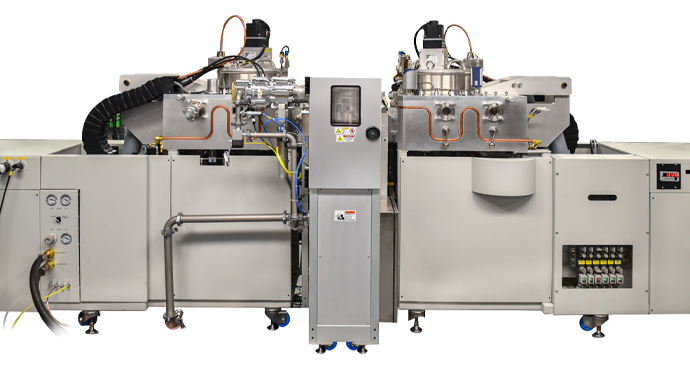
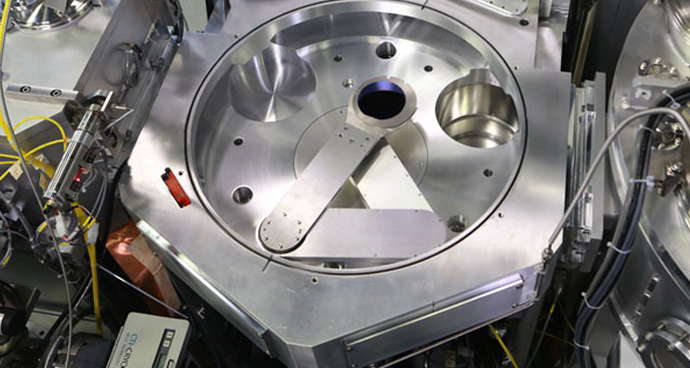
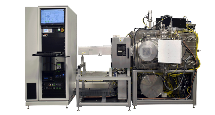
Denton’s solution to breakage due to manual handling is to automate the process as much as possible using its Versa cluster platform. Instead of having operators screw down the wafers manually in preparation for processing, they are placed in a carrier – a process that can be fully automated and performed at atmosphere – and the carrier is then loaded into the thin film system. A cassette can be used to handle up to 25 carriers at once. The operator only handles cassettes, not individual wafers. This reduces breakage and increases yield.
The Versa cluster tool can handle up to 25 cassettes in a single batch without breaking vacuum.
For more information, see How Can You Improve Factory Throughput in Thin Film Deposition?
High-mix Manufacturing, with Varying Wafer Sizes and Recipes
Many III-V semiconductor fabricators make a wide range of different wafer sizes for different applications, so their manufacturing process needs to accommodate this. This, again, is a handling issue. Most thin film systems can only handle 8-inch wafers, but the cassette-based loading system of the Denton Versa cluster tool can handle a variety of different-sized wafers without interruption.
Besides the size of the wafers, III-V manufacturers are often depositing different thin film recipes on different generations of devices. With the Versa cluster tool, Denton offers the ability to handle a variety of wafer sizes and thin-film recipes in the same batch, without breaking vacuum. This can save hours of down time over approaches that require retooling for changes in size or recipe, thus improving throughput, lowering TCO, and increasing manufacturing flexibility.
Denton’s full line of technologies – Discovery V, Discovery Isoflux, Integrity E-beam, Voyager PIB-CVD, Infinity BTS, and Infinity Ion Etch – can be paired with the Versa cluster tool.
For more information, see How to Handle Varying Wafer Sizes in Compound Semiconductor Manufacturing.
Denton and III-V Semiconductors
Denton Vacuum’s sputtering systems all feature a proprietary automated wafer carrier that can easily handle wafers of different sizes in the same system without breaking vacuum, or breaking wafers because of manual loading, answering the needs of III-V semiconductor manufacturers for the highest degree of process flexibility and scalability.
Denton offers other solutions for III-V semiconductor processes in its Infinity platform:
- Denton’s Ion Beam Etching has the ability to etch III-V materials such as silicon carbide, which is much more difficult to etch than silicon-based chips.
- Denton’s Biased Target Sputtering (BTS) offers excellent control of thin film interfaces, provides independent control over ion currents and energies, and operates at a low pressure. This results in dense, defect-free and shift-free thin films, ideal for AR/HR coatings for edge-emitting lasers and VCSELs as well as high-quality VOx IR absorbers for microbolometers. BTS can help manufacturers drive higher power from each laser, support longer useful life for each laser, and ensure repeatability for consistency in the finished product.
Conclusion
You can read more about Denton’s solutions for III-V semiconductor manufacturing here, or contact us today to discuss your particular needs.